Applied Materials Building 1
Applied Materials Building 1 - Statistical analyses were performed using modules within the monitoring and remediation optimization system software (maros) and proucl software. S a n t o m a s e x p y. Applied materials, a leader in materials engineering solutions, plays a crucial role in the semiconductor, display, and related industries. This $2,400 rental property located at 11 e illinois street #203, chicago, il 60611 has 1 bed, 1 bath and 850 sqft. 41 45a 45b 45c 35 s d ln. Our expertise in modifying materials at atomic. Is the global leader in materials engineering solutions for the semiconductor, flat panel display and solar photovoltaic (pv) industries. Located in the trendy river north. C e n t e r r i d g e d r. 4 2 6 1 3 5 7 s c o t t b l v d. $ building 41 building 45s harris branch austin, tx buildings 43 & 44 s p e c t r u m dr. In 1983, applied materials discovered that several leaks and/, spills from three onsite underground tanks near building 1 had contaminated onsite soil and shallow ground water. C e n t e r l i n e p a s s building 34 36 y w p c. Under his direction, applied is driving the flat panel display industry roadmap to enable enhanced touch panels, flexible substrates and oled displays. S a n t o m a s e x p y. Applied materials is the leader in materials engineering solutions used to produce virtually every new chip and advanced display in the world. 41 45a 45b 45c 35 s d ln. 4 2 6 1 3 5 7 s c o t t b l v d. 5 6 12 11 3 2 1 cafe parking garage main lobby entrance driveway to. Applied materials building 1 is an innovative and versatile option that has gained attention for its potential to revolutionize building practices. In this article, we will explore the. Applied materials location hotel location 85 s. Statistical analyses were performed using modules within the monitoring and remediation optimization system software (maros) and proucl software. C e n t e r r i d g e d r. Applied materials is the leader in materials engineering solutions used to produce virtually every new. Applied materials is the leader in materials engineering solutions used to produce virtually every new chip and advanced display in the world. (“applied materials”), headquartered in santa clara, california, manufactures, markets, and distributes engineering solutions and equipment used to produce. Under his direction, applied is driving the flat panel display industry roadmap to enable enhanced touch panels, flexible substrates and. 4 2 6 1 3 5 7 s c o t t b l v d. W o l f e r d e. C e n t e r r i d g e d r. Under his direction, applied is driving the flat panel display industry roadmap to enable enhanced touch panels, flexible substrates and oled displays. S. (“applied materials”), headquartered in santa clara, california, manufactures, markets, and distributes engineering solutions and equipment used to produce. In this article, we will explore the. Applied materials, a leader in materials engineering solutions, plays a crucial role in the semiconductor, display, and related industries. C e n t e r r i d g e d r. W o l. Is the global leader in materials engineering solutions for the semiconductor, flat panel display and solar photovoltaic (pv) industries. $ building 41 building 45s harris branch austin, tx buildings 43 & 44 s p e c t r u m dr. 4 2 6 1 3 5 7 s c o t t b l v d. Located in the. W o l f e r d e. Applied materials, a leader in materials engineering solutions, plays a crucial role in the semiconductor, display, and related industries. Applied materials is the leader in materials engineering solutions used to produce virtually every new chip and advanced display in the world. Statistical analyses were performed using modules within the monitoring and remediation. 41 45a 45b 45c 35 s d ln. Applied materials, a leader in materials engineering solutions, plays a crucial role in the semiconductor, display, and related industries. Applied materials is the leader in materials engineering solutions used to produce virtually every new chip and advanced display in the world. Under his direction, applied is driving the flat panel display industry. In this article, we will explore the. Located in the trendy river north. Applied materials is the leader in materials engineering solutions used to produce virtually every new chip and advanced display in the world. Applied materials is the leader in materials engineering solutions used to produce virtually every new chip and advanced display in the world. This article focuses. Applied materials, a leader in materials engineering solutions, plays a crucial role in the semiconductor, display, and related industries. Our expertise in modifying materials at atomic. Statistical analyses were performed using modules within the monitoring and remediation optimization system software (maros) and proucl software. Applied materials is the leader in materials engineering solutions used to produce virtually every new chip. Located in the trendy river north. Statistical analyses were performed using modules within the monitoring and remediation optimization system software (maros) and proucl software. Applied materials is the leader in materials engineering solutions used to produce virtually every new chip and advanced display in the world. Our expertise in modifying materials at atomic. Applied materials location hotel location 85 s. (“applied materials”), headquartered in santa clara, california, manufactures, markets, and distributes engineering solutions and equipment used to produce. Applied materials is the leader in materials engineering solutions used to produce virtually every new chip and advanced display in the world. W o l f e r d e. Our expertise in modifying materials at atomic. Applied materials building 1 is an innovative and versatile option that has gained attention for its potential to revolutionize building practices. $ building 41 building 45s harris branch austin, tx buildings 43 & 44 s p e c t r u m dr. C e n t e r r i d g e d r. Applied materials location hotel location 85 s. Applied materials, a leader in materials engineering solutions, plays a crucial role in the semiconductor, display, and related industries. 41 45a 45b 45c 35 s d ln. This article focuses on the company's. Applied materials is the leader in materials engineering solutions used to produce virtually every new chip and advanced display in the world. Our expertise in modifying materials at atomic. Under his direction, applied is driving the flat panel display industry roadmap to enable enhanced touch panels, flexible substrates and oled displays. Is the global leader in materials engineering solutions for the semiconductor, flat panel display and solar photovoltaic (pv) industries. S a n t o m a s e x p y.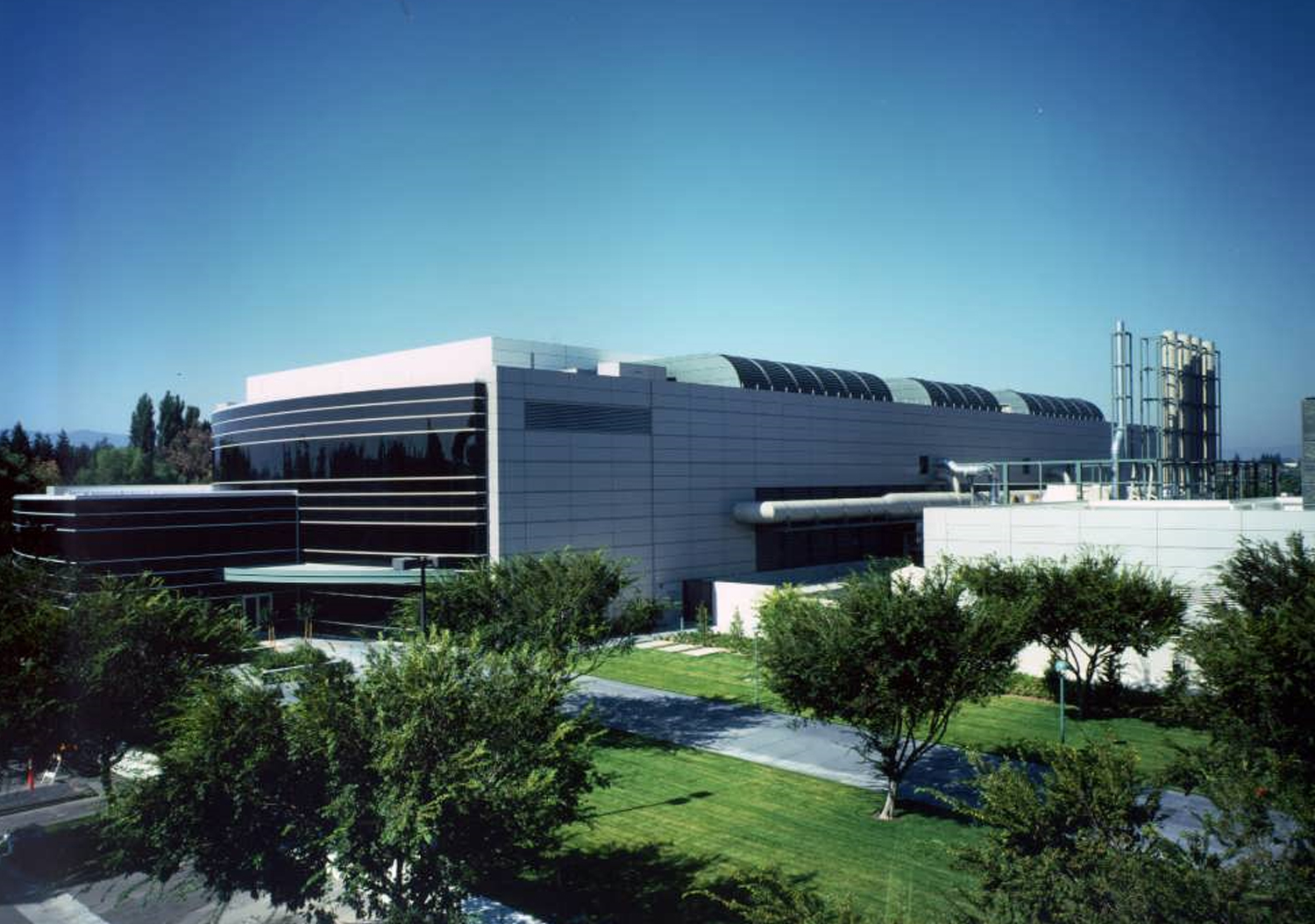
Applied Materials Arques Campus Technology Center Hathaway Dinwiddie
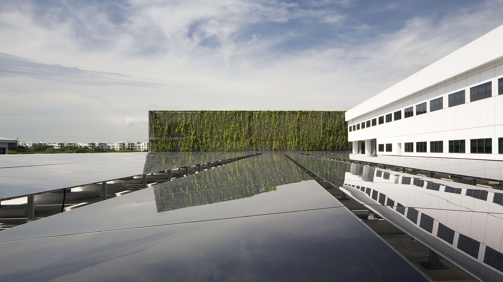
Applied Materials Building Image Singapore
Applied Materials Building By Kolker Kolker Epstein Architects LTD
Applied Materials ID Architects
Applied Materials Building Image Singapore
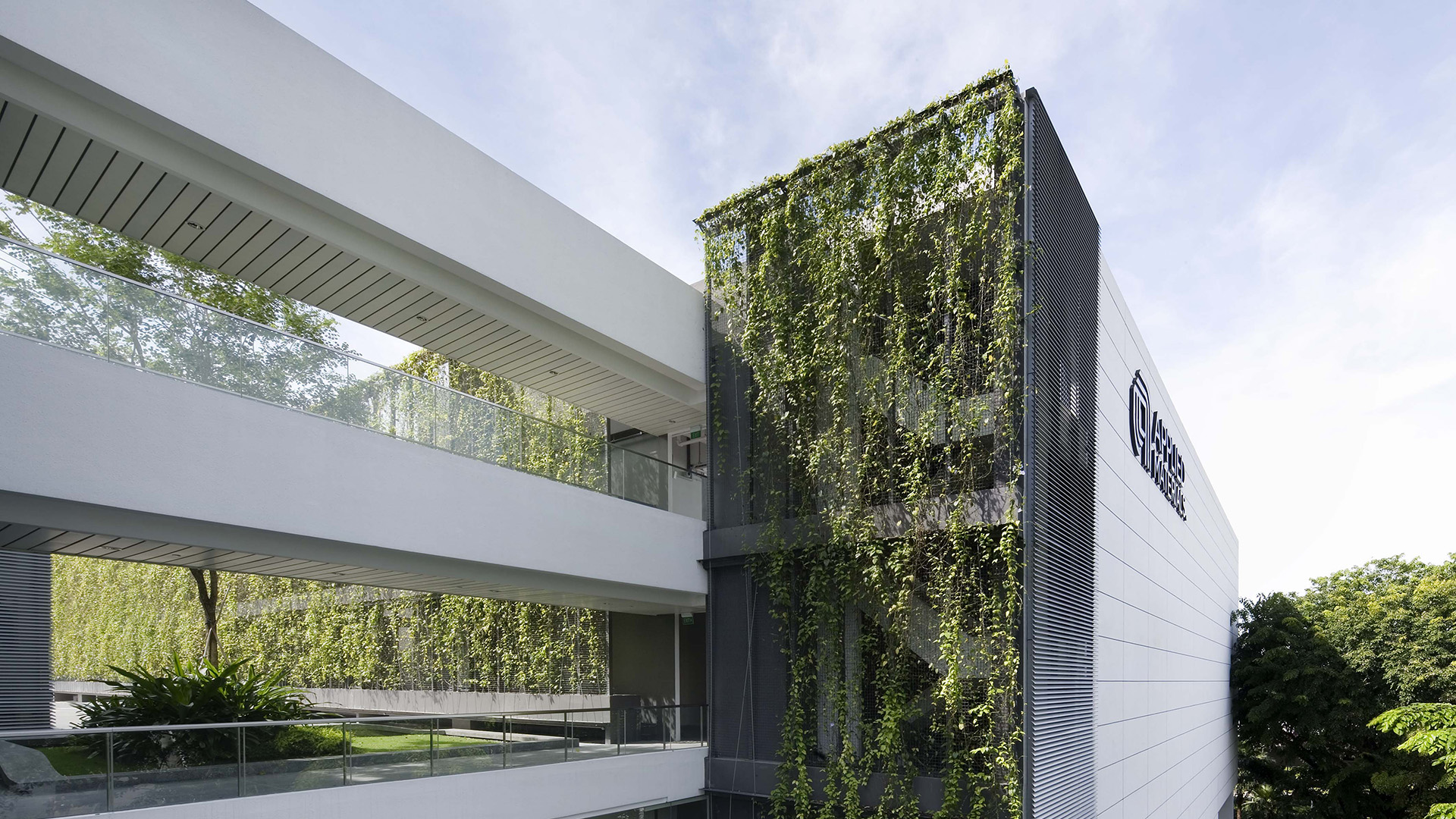
Applied Materials ID Architects
Applied Materials Building Image Singapore
Contact
Applied Materials Building By Kolker Kolker Epstein Architects LTD
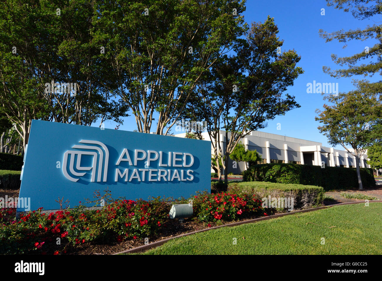
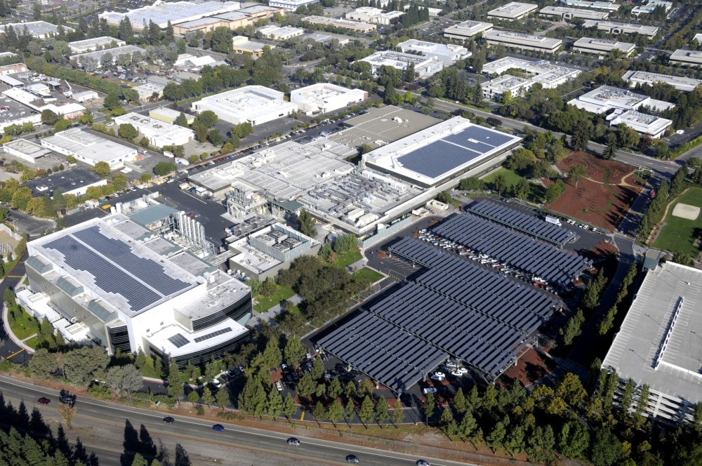
Applied Materials Inc. headquarters, Santa Clara CA Stock Photo Alamy
Located In The Trendy River North.
4 2 6 1 3 5 7 S C O T T B L V D.
This $2,400 Rental Property Located At 11 E Illinois Street #203, Chicago, Il 60611 Has 1 Bed, 1 Bath And 850 Sqft.
In This Article, We Will Explore The.
Related Post: