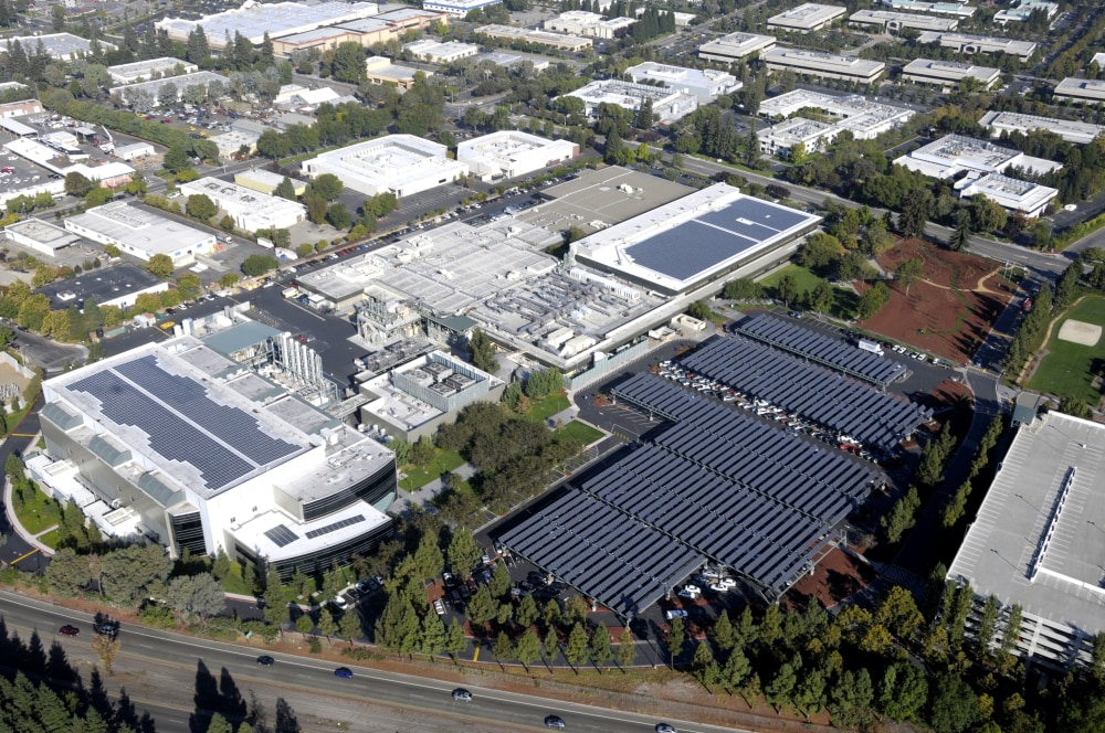
Applied Materials Building 37
Applied Materials Building 37 - Applied’s materials engineering expertise includes integrated materials solutions that combine multiple processes with customized metrology and sensors in a single system to help our. Engineered nanomaterials and other emerging materials/technologies proposed for use in areas at the. Applied materials building 37 location address: In sunnyvale, apple now rents office space from applied materials. In this article, we will explore the. Applied materials technology, products, financial news or speaking with our executives, please contact media_relations@amat.com Applied materials purchased 3 properties in sunnyvale, called arques technology center. Nalamasu has championed a renewed focus on applied’s global innovation. Is the global leader in materials engineering solutions for the semiconductor, flat panel display and solar photovoltaic (pv) industries. Applied materials building 37 is an innovative and versatile option that has gained attention for its potential to revolutionize building practices. Learn about applied materials's headquarters location and see a list of their major offices across different regions. Applied materials has announced a landmark investment to build the world’s largest and most advanced facility for collaborative semiconductor process technology and. Applied materials building 37 is an innovative and versatile option that has gained attention for its potential to revolutionize building practices. In this article, we will explore the. Engineered nanomaterials and other emerging materials/technologies proposed for use in areas at the. Today, senator daines toured kalispell’s new applied materials facility where they are manufacturing subassemblies and process equipment used in semiconductor production. On may 22, 2023, applied materials announced a landmark investment to build the world’s largest and most advanced facility for collaborative semiconductor process technology and. Is the global leader in materials engineering solutions for the semiconductor, flat panel display and solar photovoltaic (pv) industries. In sunnyvale, apple now rents office space from applied materials. Applied materials building 37 location address: Applied’s materials engineering expertise includes integrated materials solutions that combine multiple processes with customized metrology and sensors in a single system to help our. Applied materials has announced a landmark investment to build the world’s largest and most advanced facility for collaborative semiconductor process technology and. Applied materials building 37 is an innovative and versatile option that has gained attention. Engineered nanomaterials and other emerging materials/technologies proposed for use in areas at the. Find out where they operate worldwide. Learn about applied materials's headquarters location and see a list of their major offices across different regions. Applied materials building 37 location address: 9700 us 290 austin, tx 78724 location county: Applied materials purchased 3 properties in sunnyvale, called arques technology center. Engineered nanomaterials and other emerging materials/technologies proposed for use in areas at the. Applied materials building 37 location address: Today, senator daines toured kalispell’s new applied materials facility where they are manufacturing subassemblies and process equipment used in semiconductor production. Learn about applied materials's headquarters location and see a. Applied materials has announced a landmark investment to build the world’s largest and most advanced facility for collaborative semiconductor process technology and. Learn about applied materials's headquarters location and see a list of their major offices across different regions. Applied materials purchased 3 properties in sunnyvale, called arques technology center. Find out where they operate worldwide. On may 22, 2023,. Find out where they operate worldwide. 9700 us 290 austin, tx 78724 location county: Applied materials building 37 is an innovative and versatile option that has gained attention for its potential to revolutionize building practices. Applied materials building 37 location address: Applied materials purchased 3 properties in sunnyvale, called arques technology center. Learn about applied materials's headquarters location and see a list of their major offices across different regions. Applied materials building 37 location address: On may 22, 2023, applied materials announced a landmark investment to build the world’s largest and most advanced facility for collaborative semiconductor process technology and. In this article, we will explore the. 9700 us 290 austin, tx. On may 22, 2023, applied materials announced a landmark investment to build the world’s largest and most advanced facility for collaborative semiconductor process technology and. 9700 us 290 austin, tx 78724 location county: Applied materials has announced a landmark investment to build the world’s largest and most advanced facility for collaborative semiconductor process technology and. Applied materials technology, products, financial. Today, senator daines toured kalispell’s new applied materials facility where they are manufacturing subassemblies and process equipment used in semiconductor production. Is the global leader in materials engineering solutions for the semiconductor, flat panel display and solar photovoltaic (pv) industries. In this article, we will explore the. On may 22, 2023, applied materials announced a landmark investment to build the. Applied’s materials engineering expertise includes integrated materials solutions that combine multiple processes with customized metrology and sensors in a single system to help our. 9700 us 290 austin, tx 78724 location county: Is the global leader in materials engineering solutions for the semiconductor, flat panel display and solar photovoltaic (pv) industries. Applied materials purchased 3 properties in sunnyvale, called arques. Applied materials purchased 3 properties in sunnyvale, called arques technology center. 9700 us 290 austin, tx 78724 location county: On may 22, 2023, applied materials announced a landmark investment to build the world’s largest and most advanced facility for collaborative semiconductor process technology and. In sunnyvale, apple now rents office space from applied materials. Applied materials has announced a landmark. 9700 us 290 austin, tx 78724 location county: On may 22, 2023, applied materials announced a landmark investment to build the world’s largest and most advanced facility for collaborative semiconductor process technology and. Applied materials purchased 3 properties in sunnyvale, called arques technology center. Find out where they operate worldwide. Today, senator daines toured kalispell’s new applied materials facility where they are manufacturing subassemblies and process equipment used in semiconductor production. Applied materials building 37 location address: Nalamasu has championed a renewed focus on applied’s global innovation. Learn about applied materials's headquarters location and see a list of their major offices across different regions. In sunnyvale, apple now rents office space from applied materials. In this article, we will explore the. Applied materials building 37 is an innovative and versatile option that has gained attention for its potential to revolutionize building practices. Applied materials technology, products, financial news or speaking with our executives, please contact media_relations@amat.com Applied materials building 37 location address: Is the global leader in materials engineering solutions for the semiconductor, flat panel display and solar photovoltaic (pv) industries. On may 22, 2023, applied materials announced a landmark investment to build the world’s largest and most advanced facility for collaborative semiconductor process technology and.Applied Materials Building Image Singapore
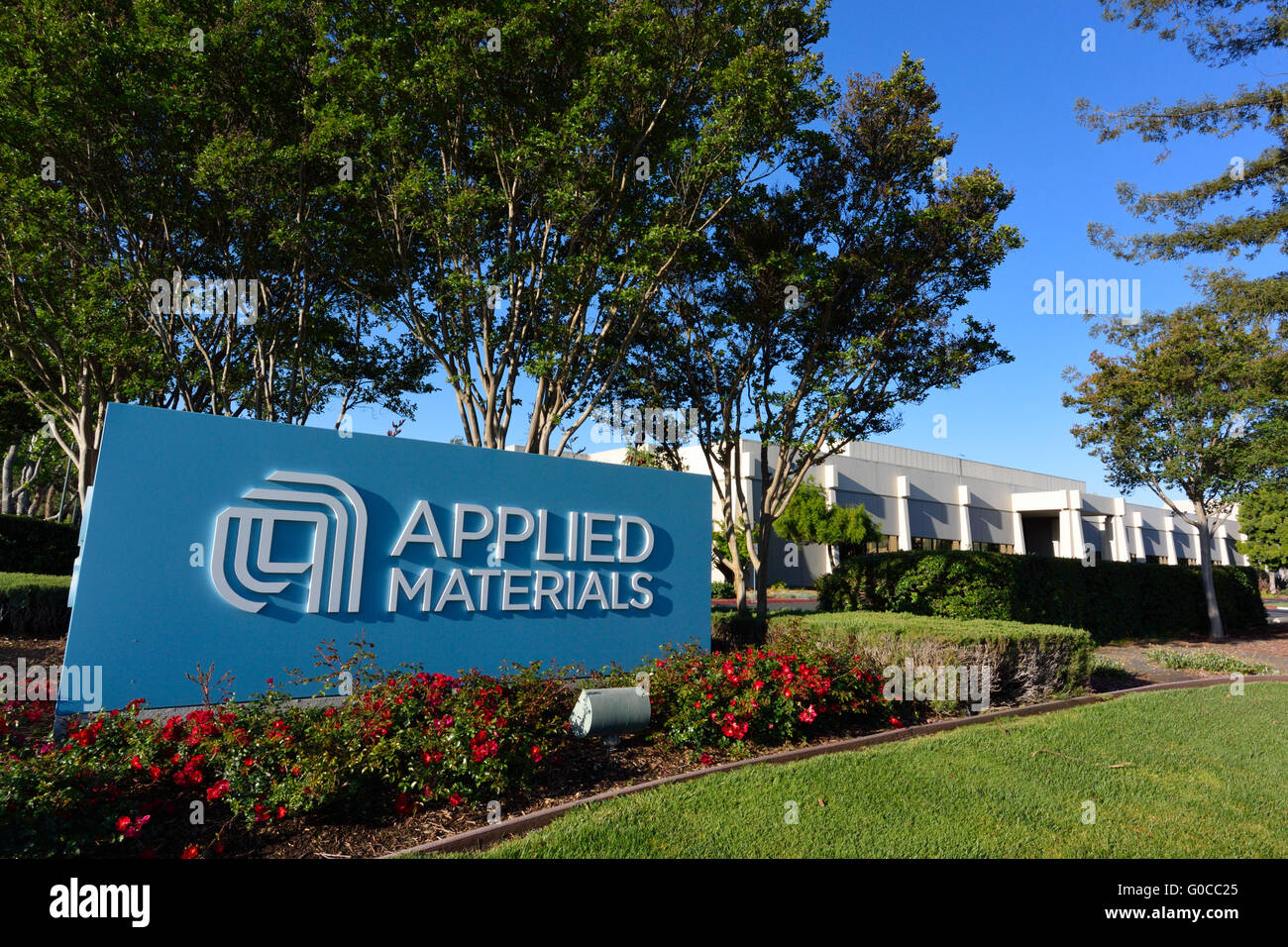
Applied Materials Inc. Hauptsitz, Santa Clara CA Stockfotografie Alamy
Applied Materials ID Architects
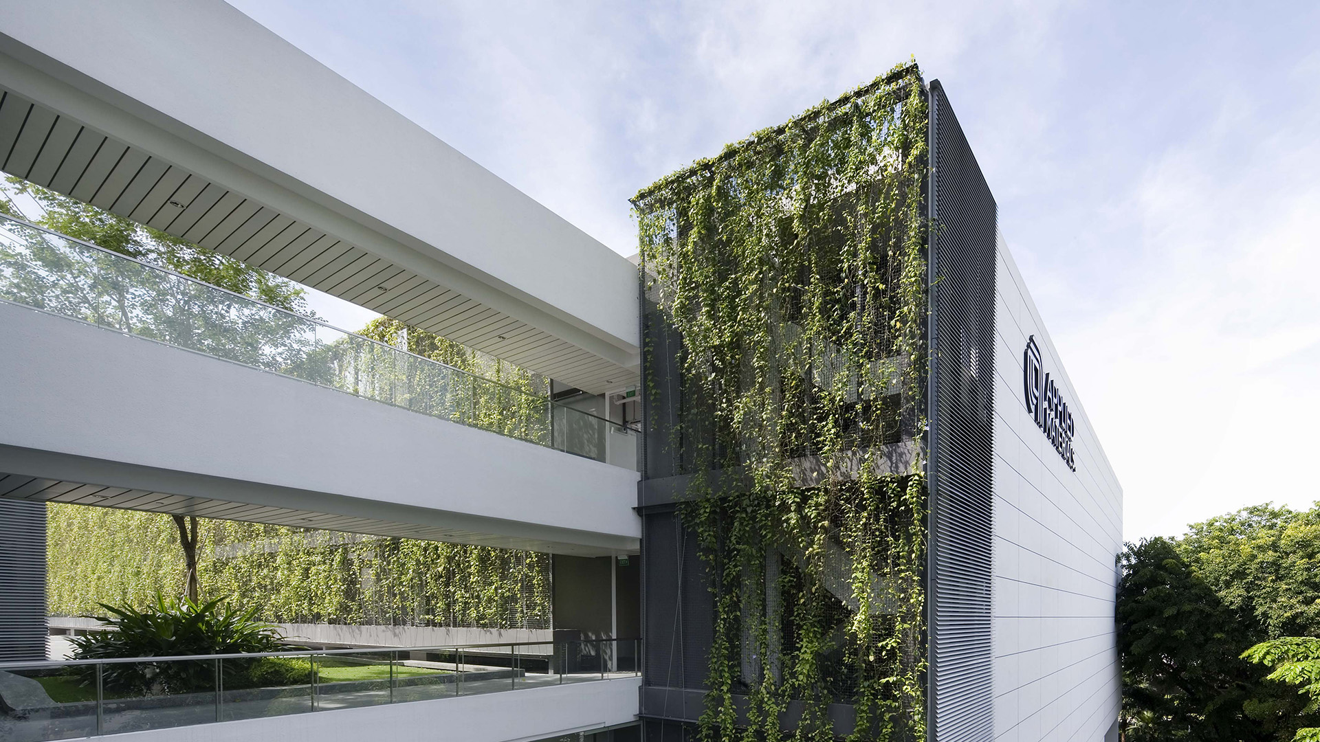
Applied Materials Building Image Singapore
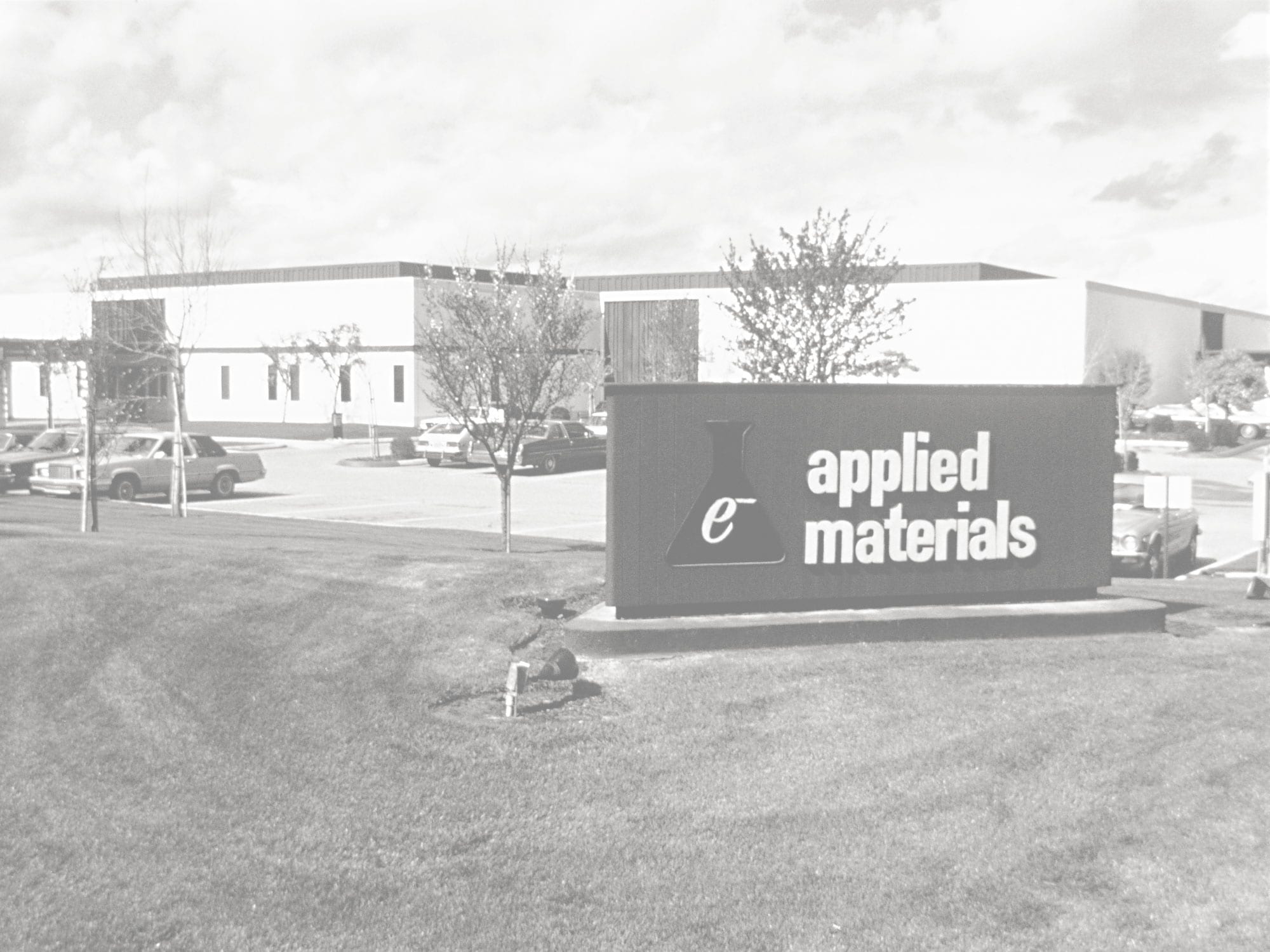
Applied Celebrates 55 Years of Technology Innovation

List of Public Semiconductors Companies in California that have
Applied Materials Building Image Singapore
Applied Materials Building By Kolker Kolker Epstein Architects LTD
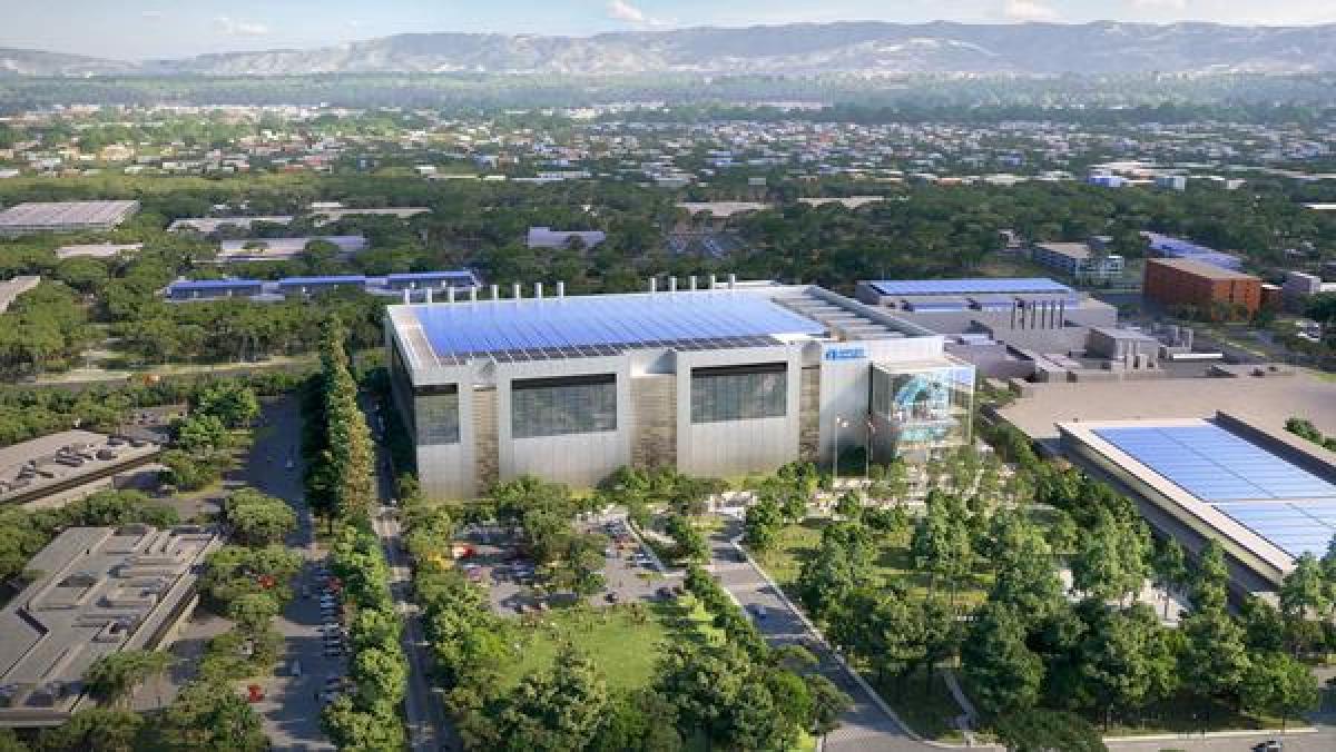
Applied Materials Plans to Build 4B Project Near HQ CEG
Contact
9700 Us 290 Austin, Tx 78724 Location County:
Applied’s Materials Engineering Expertise Includes Integrated Materials Solutions That Combine Multiple Processes With Customized Metrology And Sensors In A Single System To Help Our.
Applied Materials Has Announced A Landmark Investment To Build The World’s Largest And Most Advanced Facility For Collaborative Semiconductor Process Technology And.
Engineered Nanomaterials And Other Emerging Materials/Technologies Proposed For Use In Areas At The.
Related Post: