Applied Materials Building 52
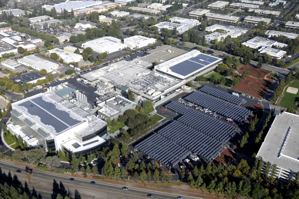
Applied Materials Building 52 - 4 2 6 1 3 5 7 s c o t t b l v d. Find out where they operate worldwide. In this article, we will explore the. Applied materials has subleased the entire office building at 3333 scott blvd. Semiconductor firm applied materials (applied) said monday that it would invest up to $4 billion into a research and development (r&d) center near its campus in santa clara, california. Semiconductor toolmaker applied materials inc on monday said it plans to spend up to $4 billion on a research center in the heart of silicon valley to speed up advances. Applied materials inc is located at 3050 bowers ave in santa clara, california 95054. Learn about applied materials santa clara, ca office. Applied materials has leased the 245k sf building 52 through 2028 5 6 12 11 3 2 1 cafe parking garage main lobby entrance driveway to. It includes 60,000 sqft of class 1 cleanroom space on 60″ deep and 45″. See reviews, salaries & interviews from applied materials employees in santa clara, ca. In this article, we will explore the. Our expertise in modifying materials at atomic. W o l f e r d e. National research council, predicting antimicrobial resistance using bacterial motility as a marker, postdoctoral research fellowship. Applied materials location hotel location 85 s. Learn about applied materials's headquarters location and see a list of their major offices across different regions. Semiconductor firm applied materials (applied) said monday that it would invest up to $4 billion into a research and development (r&d) center near its campus in santa clara, california. S a n t o m a s e x p y. It includes 60,000 sqft of class 1 cleanroom space on 60″ deep and 45″. S a n t o m a s e x p y. Semiconductor firm applied materials (applied) said monday that it would invest up to $4 billion into a research and development (r&d) center near its campus in santa clara, california. See reviews, salaries & interviews. Learn about applied materials santa clara, ca office. National research council, predicting antimicrobial resistance using bacterial motility as a marker, postdoctoral research fellowship. In this article, we will explore the. Applied materials is a global leader in materials engineering solutions, specializing in the development of advanced manufacturing technologies for the semiconductor and display. W o l f e r d. Applied materials location hotel location 85 s. Applied materials inc is located at 3050 bowers ave in santa clara, california 95054. S a n t o m a s e x p y. Learn about applied materials's headquarters location and see a list of their major offices across different regions. Applied materials has subleased the entire office building at 3333. Our expertise in modifying materials at atomic. Learn about applied materials's headquarters location and see a list of their major offices across different regions. Semiconductor toolmaker applied materials inc on monday said it plans to spend up to $4 billion on a research center in the heart of silicon valley to speed up advances. Find out where they operate worldwide.. Semiconductor toolmaker applied materials inc on monday said it plans to spend up to $4 billion on a research center in the heart of silicon valley to speed up advances. Applied materials location hotel location 85 s. Find out where they operate worldwide. Applied materials is the leader in materials engineering solutions used to produce virtually every new chip and. In this article, we will explore the. Find out where they operate worldwide. Semiconductor toolmaker applied materials inc on monday said it plans to spend up to $4 billion on a research center in the heart of silicon valley to speed up advances. Applied materials has leased the 245k sf building 52 through 2028 Semiconductor firm applied materials (applied) said. Applied materials building 52 is an innovative and versatile option that has gained attention for its potential to revolutionize building practices. Learn about applied materials's headquarters location and see a list of their major offices across different regions. Semiconductor toolmaker applied materials inc on monday said it plans to spend up to $4 billion on a research center in the. S a n t o m a s e x p y. Learn about applied materials's headquarters location and see a list of their major offices across different regions. In santa clara, california, as part of the tech company's ongoing expansion in the silicon valley. Semiconductor toolmaker applied materials inc on monday said it plans to spend up to $4. Applied materials is a global leader in materials engineering solutions, specializing in the development of advanced manufacturing technologies for the semiconductor and display. W o l f e r d e. It includes 60,000 sqft of class 1 cleanroom space on 60″ deep and 45″. 5 6 12 11 3 2 1 cafe parking garage main lobby entrance driveway to.. Applied materials has leased the 245k sf building 52 through 2028 National research council, predicting antimicrobial resistance using bacterial motility as a marker, postdoctoral research fellowship. Learn about applied materials santa clara, ca office. Semiconductor toolmaker applied materials inc on monday said it plans to spend up to $4 billion on a research center in the heart of silicon valley. S a n t o m a s e x p y. Applied materials is a global leader in materials engineering solutions, specializing in the development of advanced manufacturing technologies for the semiconductor and display. In santa clara, california, as part of the tech company's ongoing expansion in the silicon valley. Applied materials inc is located at 3050 bowers ave in santa clara, california 95054. Semiconductor firm applied materials (applied) said monday that it would invest up to $4 billion into a research and development (r&d) center near its campus in santa clara, california. Applied materials has subleased the entire office building at 3333 scott blvd. See reviews, salaries & interviews from applied materials employees in santa clara, ca. Learn about applied materials santa clara, ca office. Applied materials is the leader in materials engineering solutions used to produce virtually every new chip and advanced display in the world. Semiconductor toolmaker applied materials inc on monday said it plans to spend up to $4 billion on a research center in the heart of silicon valley to speed up advances. Our expertise in modifying materials at atomic. Applied materials has leased the 245k sf building 52 through 2028 It includes 60,000 sqft of class 1 cleanroom space on 60″ deep and 45″. In this article, we will explore the. 5 6 12 11 3 2 1 cafe parking garage main lobby entrance driveway to. Applied materials building 52 is an innovative and versatile option that has gained attention for its potential to revolutionize building practices.
Building 52 Materials Summary Text Hastingson
Applied Materials Inc. Hauptsitz, Santa Clara CA Stockfotografie Alamy
Applied Materials Building Image Singapore
Applied Materials Building Image Singapore
Applied Materials ID Architects
Applied Materials Building Image Singapore
Applied Materials Building By Kolker Kolker Epstein Architects LTD
Amat applied materials hires stock photography and images Alamy
Contact
Applied Materials Building By Kolker Kolker Epstein Architects LTD
W O L F E R D E.
National Research Council, Predicting Antimicrobial Resistance Using Bacterial Motility As A Marker, Postdoctoral Research Fellowship.
4 2 6 1 3 5 7 S C O T T B L V D.
Find Out Where They Operate Worldwide.
Related Post: