Applied Materials Building 74
Applied Materials Building 74 - 32 is a building in travis, texas which is located on us 290 east. W o l f e r d e. Learn about applied materials's headquarters location and see a list of their major offices across different regions. Amat) disclosed an investment of around $4 billion for creating the world's largest and most highly advanced research facility, equipment and process. Find out where they operate worldwide. The global semiconductor equipment company redefined many of its building and assembly standards in the planning of this manufacturing center, led by graeber, simmons and cowan. S a n t o m a s e x p y. 32 is situated nearby to real hope church , as well as near the motorhome. 5 6 12 11 3 2 1 cafe parking garage main lobby entrance driveway to. On may 22, 2023, applied materials announced a landmark investment to build the world’s largest and most advanced facility for collaborative semiconductor process technology and. 32 is situated nearby to real hope church , as well as near the motorhome. Learn about applied materials's headquarters location and see a list of their major offices across different regions. S a n t o m a s e x p y. 5 6 12 11 3 2 1 cafe parking garage main lobby entrance driveway to. Semiconductor firm applied materials (applied) said monday that it would invest up to $4 billion into a research and development (r&d) center near its campus in santa clara, california. Find out where they operate worldwide. 32 is a building in travis, texas which is located on us 290 east. The global semiconductor equipment company redefined many of its building and assembly standards in the planning of this manufacturing center, led by graeber, simmons and cowan. Amat) disclosed an investment of around $4 billion for creating the world's largest and most highly advanced research facility, equipment and process. Applied materials location hotel location 85 s. Vice president kamala harris' visit comes as a silicon valley tech giant, applied materials, announced it plans to build a $4 billion semiconductor research and development. S a n t o m a s e x p y. 32 is situated nearby to real hope church , as well as near the motorhome. Semiconductor firm applied materials (applied) said monday. S a n t o m a s e x p y. Find out where they operate worldwide. Applied materials, the biggest maker of machines for producing semiconductors, said on monday that it planned to build a massive research facility near its hometown, santa. 5 6 12 11 3 2 1 cafe parking garage main lobby entrance driveway to. Semiconductor. Semiconductor firm applied materials (applied) said monday that it would invest up to $4 billion into a research and development (r&d) center near its campus in santa clara, california. 32 is a building in travis, texas which is located on us 290 east. On may 22, 2023, applied materials announced a landmark investment to build the world’s largest and most. Vice president kamala harris' visit comes as a silicon valley tech giant, applied materials, announced it plans to build a $4 billion semiconductor research and development. Amat) disclosed an investment of around $4 billion for creating the world's largest and most highly advanced research facility, equipment and process. 32 is situated nearby to real hope church , as well as. S a n t o m a s e x p y. Applied materials, the biggest maker of machines for producing semiconductors, said on monday that it planned to build a massive research facility near its hometown, santa. Amat) disclosed an investment of around $4 billion for creating the world's largest and most highly advanced research facility, equipment and process.. Sunnyvale — applied materials has bought two sunnyvale research buildings, an indication that the tech titan has yet to quench its thirst for silicon valley buildings that it. On may 22, 2023, applied materials announced a landmark investment to build the world’s largest and most advanced facility for collaborative semiconductor process technology and. 32 is a building in travis, texas. Semiconductor toolmaker applied materials inc on monday said it plans to spend up to $4 billion on a research center in the heart of silicon valley to speed up advances. Applied materials, the biggest maker of machines for producing semiconductors, said on monday that it planned to build a massive research facility near its hometown, santa. 32 is situated nearby. The global semiconductor equipment company redefined many of its building and assembly standards in the planning of this manufacturing center, led by graeber, simmons and cowan. 4 2 6 1 3 5 7 s c o t t b l v d. 32 is situated nearby to real hope church , as well as near the motorhome. Sunnyvale — applied. Amat) disclosed an investment of around $4 billion for creating the world's largest and most highly advanced research facility, equipment and process. Semiconductor firm applied materials (applied) said monday that it would invest up to $4 billion into a research and development (r&d) center near its campus in santa clara, california. Applied materials location hotel location 85 s. Sunnyvale —. Sunnyvale — applied materials has bought two sunnyvale research buildings, an indication that the tech titan has yet to quench its thirst for silicon valley buildings that it. On may 22, 2023, applied materials announced a landmark investment to build the world’s largest and most advanced facility for collaborative semiconductor process technology and. Vice president kamala harris' visit comes as. Vice president kamala harris' visit comes as a silicon valley tech giant, applied materials, announced it plans to build a $4 billion semiconductor research and development. Learn about applied materials's headquarters location and see a list of their major offices across different regions. Semiconductor toolmaker applied materials inc on monday said it plans to spend up to $4 billion on a research center in the heart of silicon valley to speed up advances. S a n t o m a s e x p y. 32 is situated nearby to real hope church , as well as near the motorhome. Find out where they operate worldwide. Semiconductor firm applied materials (applied) said monday that it would invest up to $4 billion into a research and development (r&d) center near its campus in santa clara, california. Applied materials location hotel location 85 s. W o l f e r d e. The global semiconductor equipment company redefined many of its building and assembly standards in the planning of this manufacturing center, led by graeber, simmons and cowan. Amat) disclosed an investment of around $4 billion for creating the world's largest and most highly advanced research facility, equipment and process. Applied materials, the biggest maker of machines for producing semiconductors, said on monday that it planned to build a massive research facility near its hometown, santa. On may 22, 2023, applied materials announced a landmark investment to build the world’s largest and most advanced facility for collaborative semiconductor process technology and.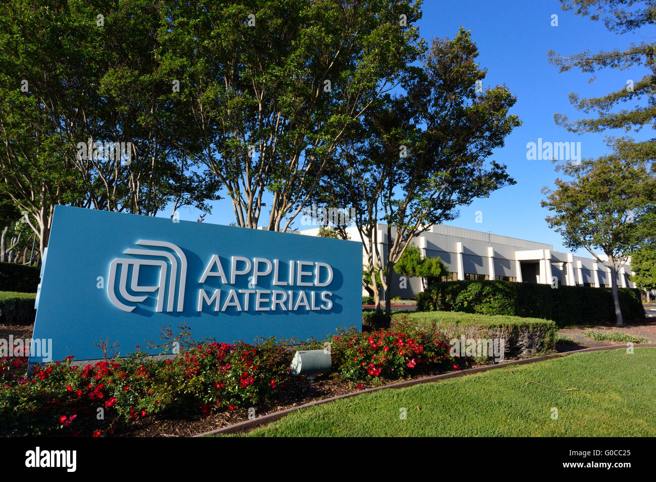
Applied Materials Inc. Hauptsitz, Santa Clara CA Stockfotografie Alamy
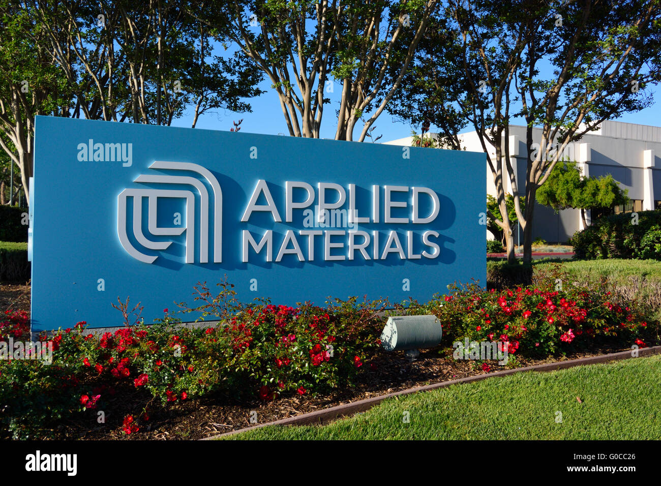
Applied Materials Inc. headquarters, Santa Clara CA Stock Photo Alamy
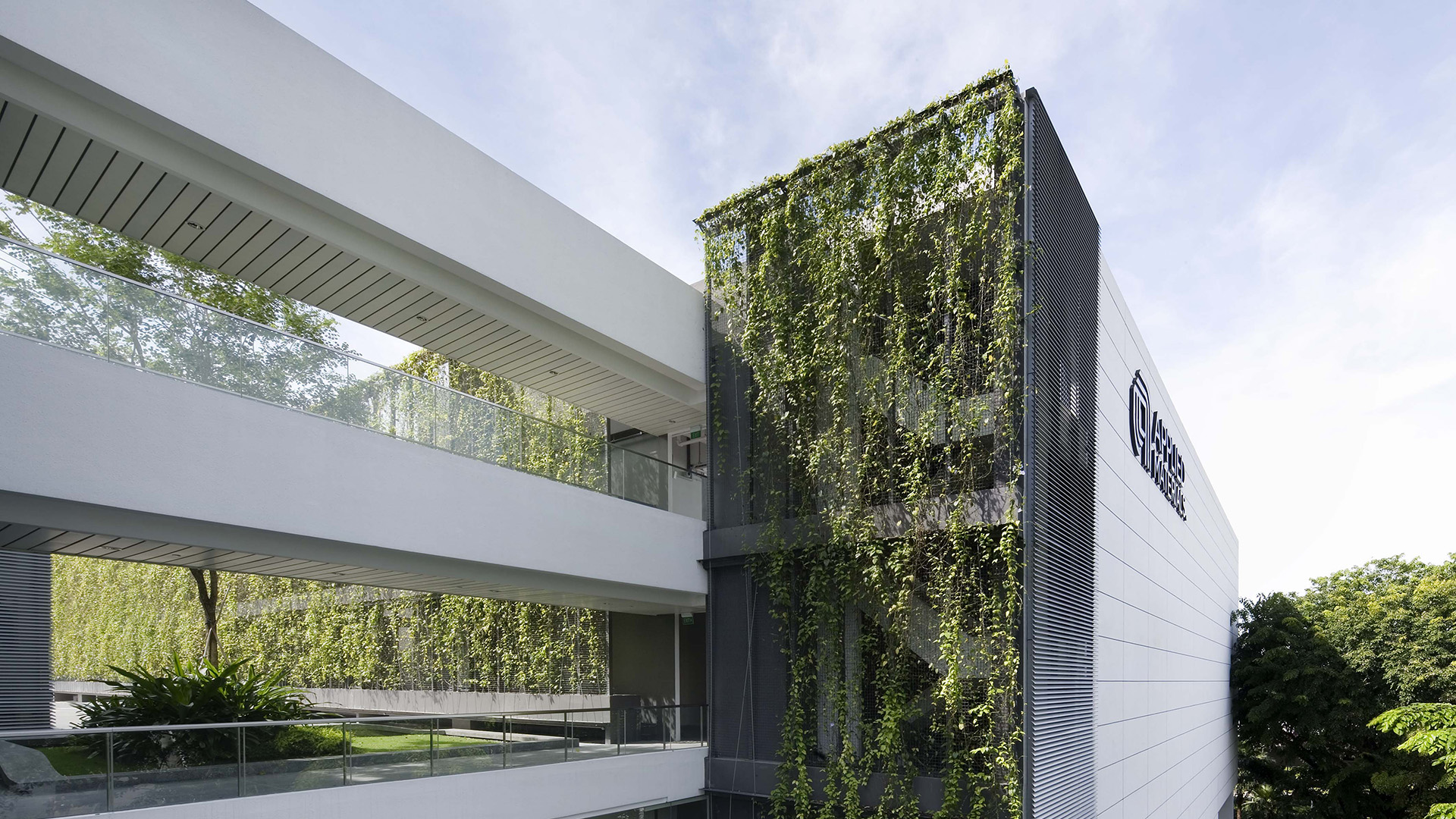
Applied Materials Building Image Singapore
Contact
Applied Materials Building Image Singapore

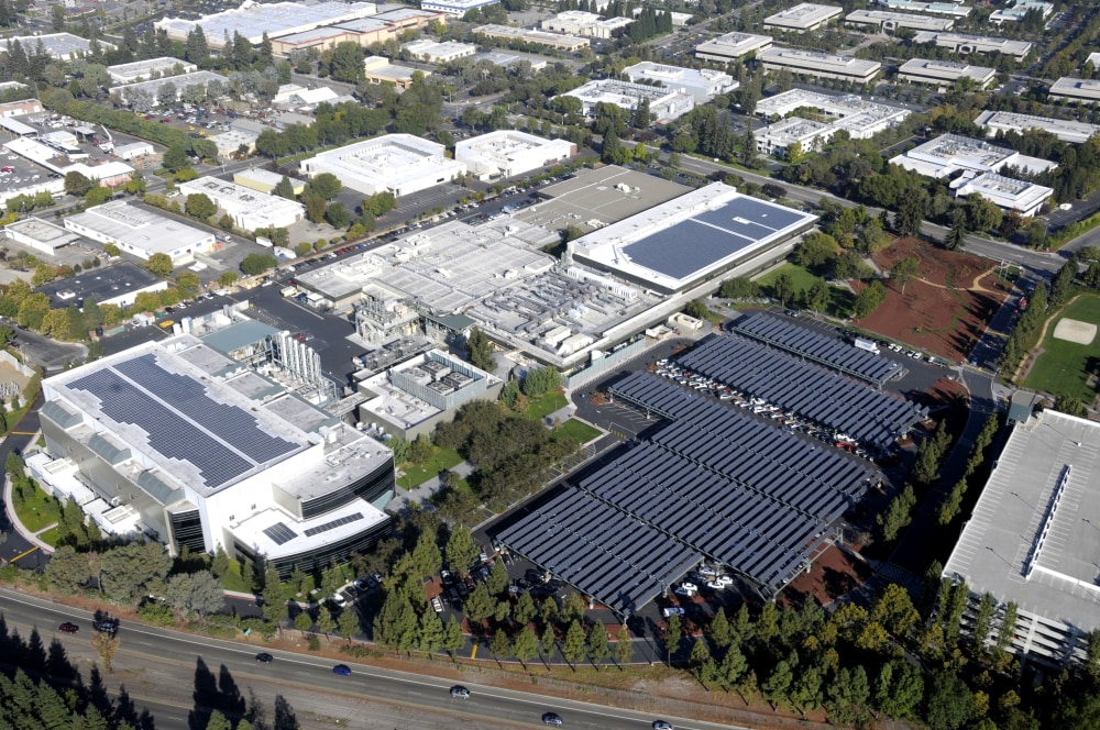
Applied Materials Sunnyvale property shopping cart tops 190 million
Applied Materials Building Image Singapore

Applied Materials Office Photos Glassdoor
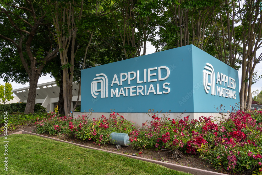
Foto de Applied Materials ground sign outside of their corporate campus
Applied Materials ID Architects
4 2 6 1 3 5 7 S C O T T B L V D.
5 6 12 11 3 2 1 Cafe Parking Garage Main Lobby Entrance Driveway To.
32 Is A Building In Travis, Texas Which Is Located On Us 290 East.
Sunnyvale — Applied Materials Has Bought Two Sunnyvale Research Buildings, An Indication That The Tech Titan Has Yet To Quench Its Thirst For Silicon Valley Buildings That It.
Related Post: