How To Build A Footprint Altium
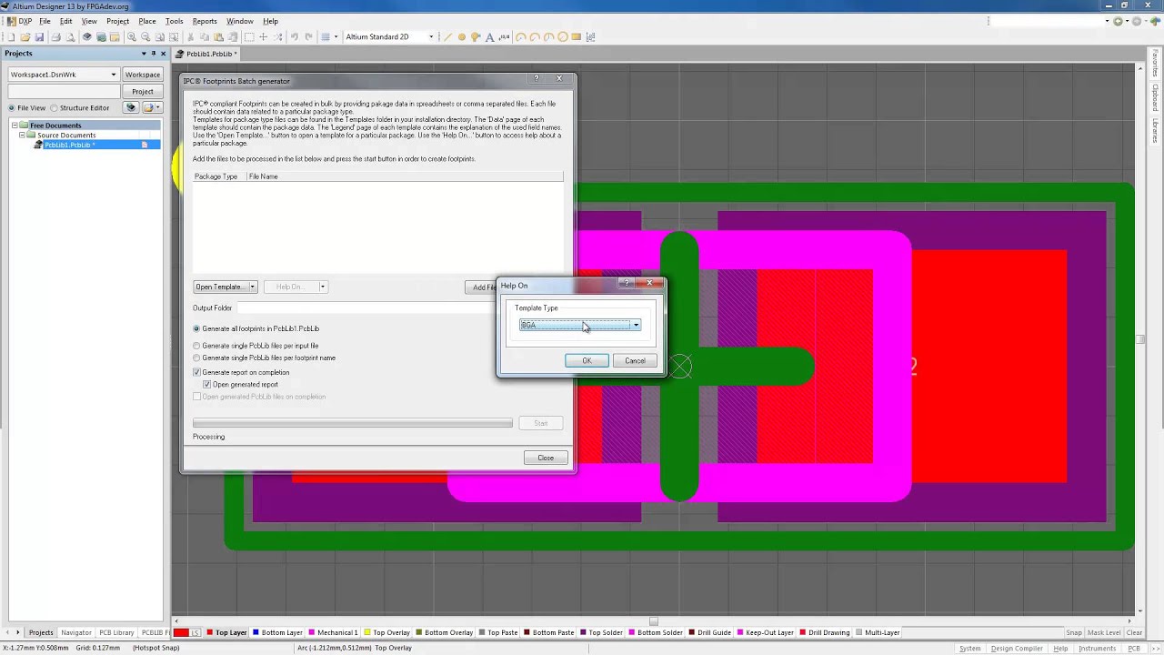
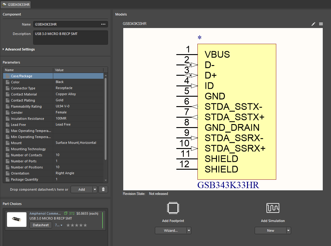
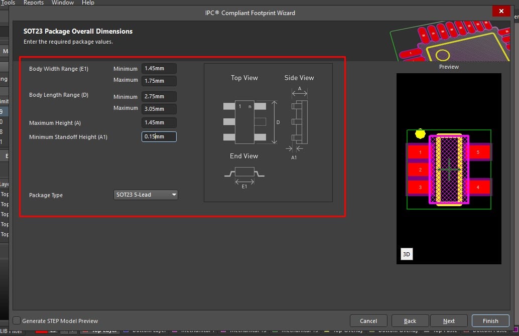
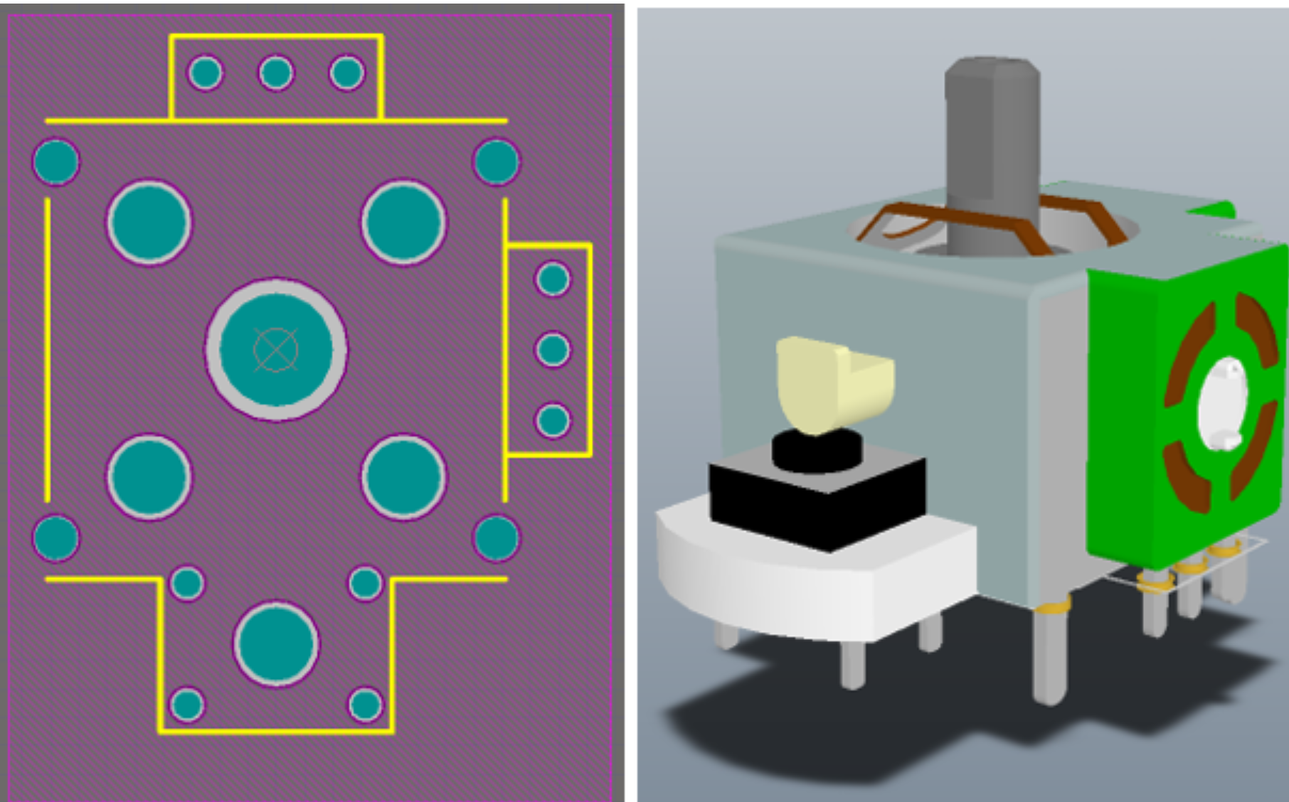
How To Build A Footprint Altium - Here’s how to create your footprint in altium designer in 4 easy steps: Pcb component footprints are created in the pcb library editor using the same set of primitive objects available in the pcb editor. In addition to footprints, company logos,. This page looks at creating a pcb footprint, which defines the place on the pcb where the physical component mounts and connects. In this tutorial, you will learn how to create a pcb component footprint in kicad, allegro, and altium designer. This video will show you how to design a schematic and pcb footprint for a specific chip of your choice. The footprint is created from a set of. This article explains how to choose one of four ways (ipc compliant wizard, batch generator, component wizard or manual) of creating a footprint (land pattern) in altium designer. This is done in altium designer, but in other softwa. Altium designer is a popular software used by engineers and designers to create printed circuit board designs. Altium designer is a popular software used by engineers and designers to create printed circuit board designs. In addition to footprints, company logos,. Here’s how to create your footprint in altium designer in 4 easy steps: In this tutorial, you will learn how to create a pcb component footprint in kicad, allegro, and altium designer. #altium #pcb #electronicstutorial in this video, we look at how to create a footprint using the latest altium designer 20.more. One of the key aspects of pcb design is creating custom. Pcb component footprints are created in the pcb library editor using the same set of primitive objects available in the pcb editor. This article explains how to choose one of four ways (ipc compliant wizard, batch generator, component wizard or manual) of creating a footprint (land pattern) in altium designer. This is done in altium designer, but in other softwa. In this video you will learn how to design own footprint in altium designer in pcb design in altium,, after watching this video you will be able to create own footprint in altium. You will need the landing pattern for your part, which can be found towards the end of the component. In this tutorial, you will learn how to create a pcb component footprint in kicad, allegro, and altium designer. #altium #pcb #electronicstutorial in this video, we look at how to create a footprint using the latest altium designer 20.more. This page. Pcb component footprints are created in the pcb library editor using the same set of primitive objects available in the pcb editor. Here’s how to create your footprint in altium designer in 4 easy steps: The footprint is created from a set of. This article explains how to choose one of four ways (ipc compliant wizard, batch generator, component wizard. This page looks at creating a pcb footprint, which defines the place on the pcb where the physical component mounts and connects. The footprint is created from a set of. #altium #pcb #electronicstutorial in this video, we look at how to create a footprint using the latest altium designer 20.more. In this tutorial, you will learn how to create a. Altium designer is a popular software used by engineers and designers to create printed circuit board designs. This article explains how to choose one of four ways (ipc compliant wizard, batch generator, component wizard or manual) of creating a footprint (land pattern) in altium designer. One of the key aspects of pcb design is creating custom. #altium #pcb #electronicstutorial in. This is done in altium designer, but in other softwa. Pcb component footprints are created in the pcb library editor using the same set of primitive objects available in the pcb editor. In this video you will learn how to design own footprint in altium designer in pcb design in altium,, after watching this video you will be able to. This is done in altium designer, but in other softwa. This article explains how to choose one of four ways (ipc compliant wizard, batch generator, component wizard or manual) of creating a footprint (land pattern) in altium designer. You will need the landing pattern for your part, which can be found towards the end of the component. This page looks. In this tutorial, you will learn how to create a pcb component footprint in kicad, allegro, and altium designer. This article explains how to choose one of four ways (ipc compliant wizard, batch generator, component wizard or manual) of creating a footprint (land pattern) in altium designer. This video will show you how to design a schematic and pcb footprint. This page looks at creating a pcb footprint, which defines the place on the pcb where the physical component mounts and connects. Why create pcb component footprints? The footprint is created from a set of. Pcb component footprints are created in the pcb library editor using the same set of primitive objects available in the pcb editor. This is done. Pcb component footprints are created in the pcb library editor using the same set of primitive objects available in the pcb editor. The footprint is created from a set of. Here’s how to create your footprint in altium designer in 4 easy steps: You will need the landing pattern for your part, which can be found towards the end of. Altium designer is a popular software used by engineers and designers to create printed circuit board designs. This page looks at creating a pcb footprint, which defines the place on the pcb where the physical component mounts and connects. In addition to footprints, company logos,. One of the key aspects of pcb design is creating custom. This video will show. This video will show you how to design a schematic and pcb footprint for a specific chip of your choice. In addition to footprints, company logos,. Here’s how to create your footprint in altium designer in 4 easy steps: Pcb component footprints are created in the pcb library editor using the same set of primitive objects available in the pcb editor. In this tutorial, you will learn how to create a pcb component footprint in kicad, allegro, and altium designer. In this video you will learn how to design own footprint in altium designer in pcb design in altium,, after watching this video you will be able to create own footprint in altium. This page looks at creating a pcb footprint, which defines the place on the pcb where the physical component mounts and connects. This article explains how to choose one of four ways (ipc compliant wizard, batch generator, component wizard or manual) of creating a footprint (land pattern) in altium designer. Altium designer is a popular software used by engineers and designers to create printed circuit board designs. You will need the landing pattern for your part, which can be found towards the end of the component. This is done in altium designer, but in other softwa. One of the key aspects of pcb design is creating custom.
How To Make A Footprint In Altium
How To Create Footprint In Altium

Arduino Mega Altium Footprint

How to Import 3D STEP model into footprint in Altium Designer YouTube

How to make a footprint for a TP4056 module in Altium Designer YouTube
Manual Footprint Creation in Altium 365 Library Management Video
PCB Design Course Altium Designer Footprint Creation Tutorial
4 Steps on How to Create a Component Footprint in Altium Designer

How To Make Footprint In Altium Designer at David Leroy blog

Pads length in Altium footprint wizard Electrical Engineering Stack
Why Create Pcb Component Footprints?
The Footprint Is Created From A Set Of.
#Altium #Pcb #Electronicstutorial In This Video, We Look At How To Create A Footprint Using The Latest Altium Designer 20.More.
Related Post: